
🔔 Read us on Telegram — don’t miss the latest automotive news → t.me/motorhub_en
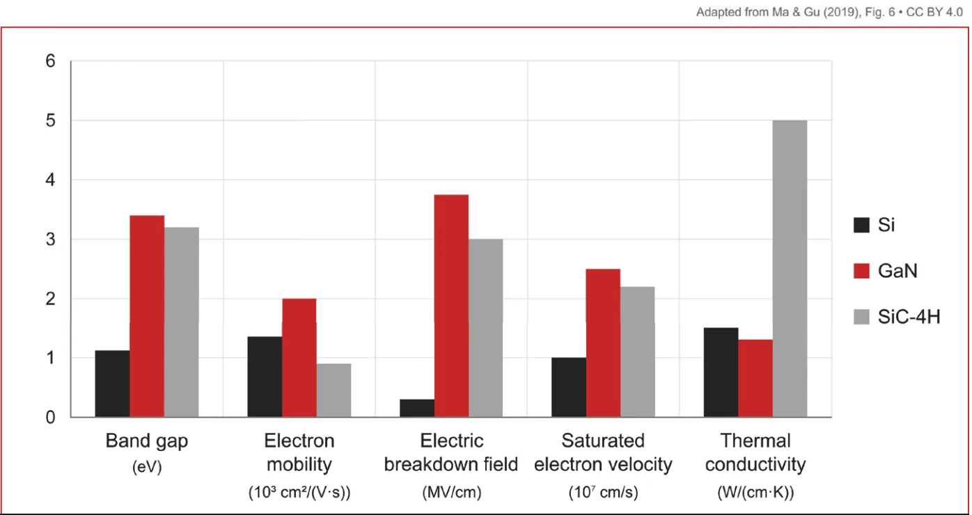
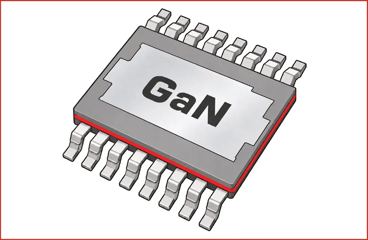
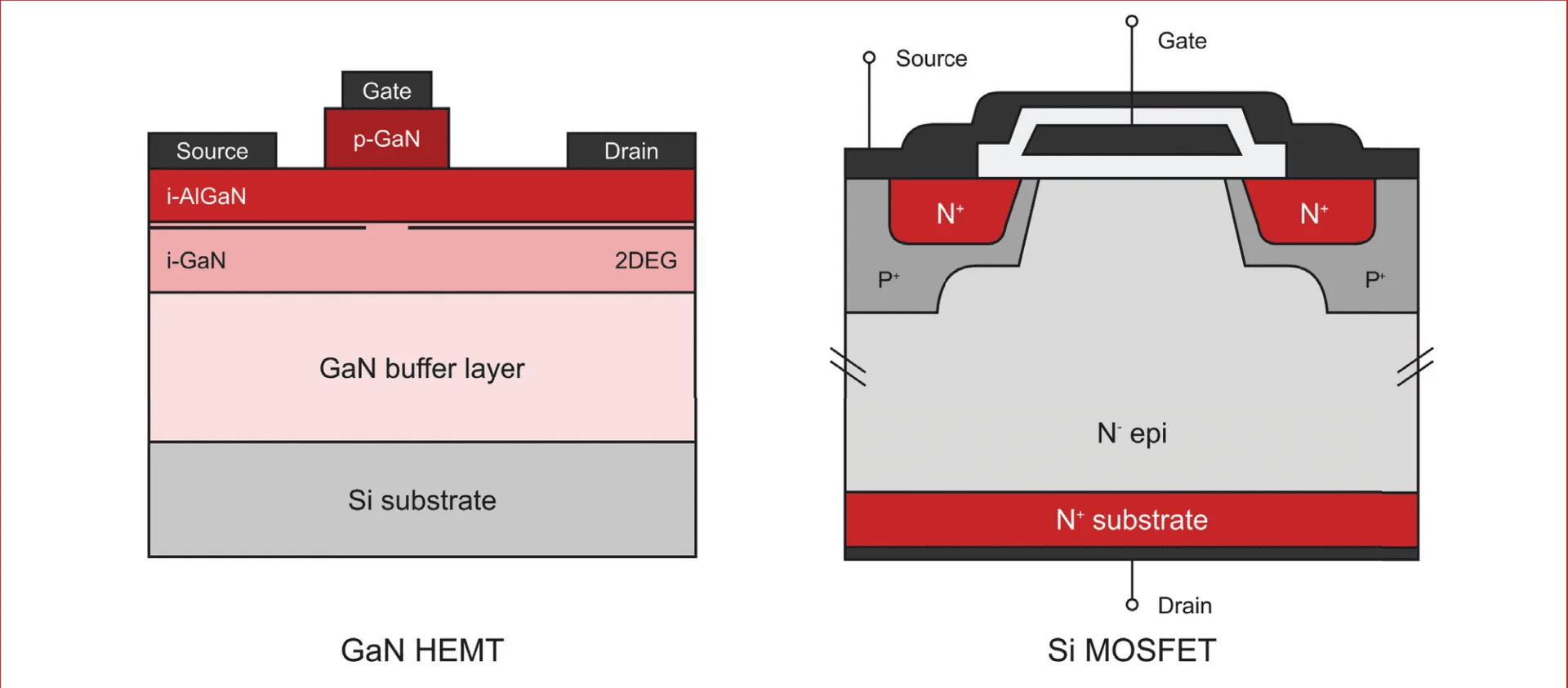
GaN switches have been gaining market share over conventional silicon counterparts due to their lower total losses at higher switching frequencies and power levels. However, GaN switches can be constructed in numerous ways, with differing behaviors between them.
SiC MOSFETs behave more or less the same as their conventional Si counterparts, but GaN has its advantages, particularly in its blazing fast switching speed and lower parasitic capacitances.
GaN switches can typically withstand a surprising amount of overvoltage without avalanching, but they tend to have a very anemic pulse current rating.
The different approaches to enabling enhancement-mode behavior in GaN switches have resulted in a diverse range of gate drive requirements.
To actually make use of GaN’s extreme speed—and to realize its promise of lower switching losses—requires even more care than usual in minimizing loop inductances.
GaN is very compelling whenever minimizing the volume and/or weight of reactive energy storage components from a massive increase in switching frequency is a high priority, such as an onboard charger or DC/DC converter.
However, GaN would be a poor fit in the traction inverter, with its relatively low pulse current capability and faster switching speed being a negative.
Technical superiority is irrelevant if you can’t get the same part number—or a drop-in substitute—a year or two from now, and GaN does seem to be uniquely susceptible to this problem.


📱 Follow our Telegram channel for daily updates
Source: Charged EVs